American standard lap joint flange production implemented strictly in accordance with ANSI, the main materials are: carbon steel, stainless steel, alloy steel.American standard lap joint flange is mainly used in pressure vessel, oil and gas pipeline engineering, pipeline engineering, chemical plants, municipal engineering, sewage treatment, power plant, shipbuilding, pharmaceutical, dairy products, beer, beverage, water conservancy and other industries.American standard lap joint flange product quality through ISO9001:2008 quality management system certification, ISO14001 environmental management system certification, OHSAS18001 occupational health and safety management system, special equipment manufacturing license pressure pipes. ANSI Standard Flange, ANSI Flange, ANSI 150 Flange, ANSI B16.5 Flange Hebei Jimeng Highstrength Flange-tubes Group Co.,Ltd. , https://www.jimengflange.com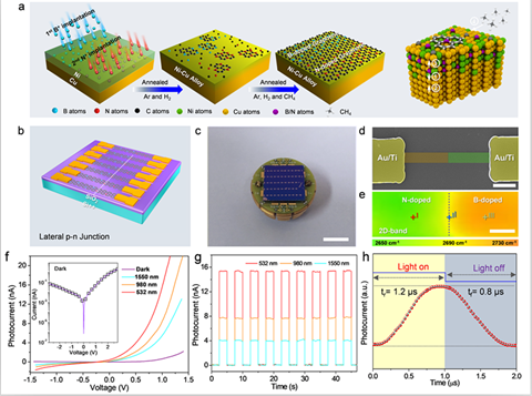
[ China Instrument Network Instrument Development ] Traditional semiconductor pn heterojunction is the core structure of bipolar transistors and field effect transistors, and is the basis of modern integrated circuit technology. Similarly, the construction of graphene pn heterojunctions is also the key to the development of graphene-based integrated circuits and photodetection technologies in the future.
Due to the limitation of the monoatomic layer thickness of the graphene material, it is difficult to achieve controlled doping of the graphene material by the ion implantation technique in the conventional integrated circuit manufacturing process. In addition, techniques such as in-situ growth doping and chemical modification doping are difficult to achieve the doping doping required for pn heterojunction. Therefore, there are challenges in achieving controllable doping of graphene (doping species, concentration, and region) and building high quality graphene pn heterojunction arrays.
The High-end Silicon-based Materials and Applications Group of the State Key Laboratory of Information Functional Materials of the Shanghai Institute of Microsystems, Chinese Academy of Sciences, has made significant progress in the array preparation and photodetection of high-quality graphene pn heterojunctions. Researchers such as Di Zengfeng and Wang Gang combined with ion implantation and chemical vapor deposition (CVD) techniques to prepare precise doped graphene materials using a two-step kinetic path of “heteroatomic nucleation-promoting graphene regrowthâ€.
By controlling the type and dose of implanted ions, n-type and p-type graphene with precise doping concentration are realized; by selective implantation, n-type dopant ions and p-type doping are stepwise implanted in adjacent regions of the same substrate. Ion, successfully constructed a horizontal graphene pn heterojunction array. The graphene pn heterojunction array has excellent photodetection performance, and its response degree is 1.4~4.7 AW-1, and the detection rate reaches ~1012 cmHz1/2W-1. This research provides a solution for the development of low-cost, large-scale, high-efficiency graphene photodetectors, which is expected to promote the scale application of graphene materials in the field of photodetection.
Related research results were published on Nature Communications, September 5, 2018, under the title "Seamless lateral graphene pn junctions formed by selective in situ doping for high-performance photodetectors" (Nature Communications, 9, 5168 (2018)).
The work was supported by the National Science and Technology Major Project, the National Natural Science Foundation, the Frontier Science Key Research Project of the Chinese Academy of Sciences, the Strategic Pilot Science and Technology Project of the Chinese Academy of Sciences, and the Shanghai Academic/Technical Leadership Program.
(Original title: Important progress in the construction of horizontal graphene pn heterojunction arrays and their photodetection research in Shanghai Microsystems)